
Cross-Sectional Analysis for Electronic Devices

Volatile Organic Compounds (VOCs)
May 13, 2026
C3 New service : Special Offer 2,000 baht
May 14, 2026Cross-Sectional Analysis for Electronic Devices

Cross-Sectional Analysis for Electronic Devices: Seeing What the Naked Eye Can’t
When the Real Problem Is Hidden Inside
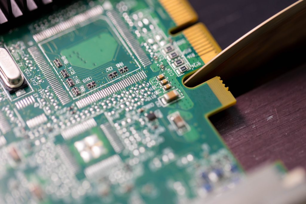
In electronics manufacturing, the most critical defects are often the ones you can’t see. A hairline crack in a solder joint, a void in a plating layer, an invisible delamination between PCB layers — any of these can cause a device to fail unpredictably in the field, with consequences ranging from product recalls to safety incidents.
Cross-sectional analysis is the technique that makes the invisible visible. By physically sectioning a component and examining its internal structure with precision instruments, engineers gain access to information that no surface inspection can provide — and that information is often the difference between a reliable product and an expensive failure.
What Is Cross-Sectional Analysis — and Why Does It Matter?
Cross-sectional analysis involves preparing a material or device specimen by cutting, mounting, and polishing it to reveal a precise internal cross-section, then examining that section under high-powered microscopy. It’s routinely applied to PCBs, PCBAs (assembled boards), integrated circuits (ICs), and a wide range of other electronic and industrial components.
The Five Core Objectives
Table
| Objective | What It Delivers |
|---|---|
| Defect Detection | Identifies incomplete connections, solder defects, and structural flaws before they cause failures in the field |
| Material Quality Assessment | Evaluates layer thickness, density, mechanical strength, and durability — informing better material selection decisions |
| Failure Analysis | Traces the root cause of device failures with scientific precision, not guesswork |
| Product Development | Reveals weaknesses in current designs and provides the data needed to build better, more reliable products |
| Cost Reduction | Catching defects early in production is dramatically cheaper than recalls, rework, or warranty claims downstream |
Step-by-Step: The Cross-Sectional Analysis Process
Reliable results depend on rigorous, standardized preparation. Here’s how the process unfolds at ALS:
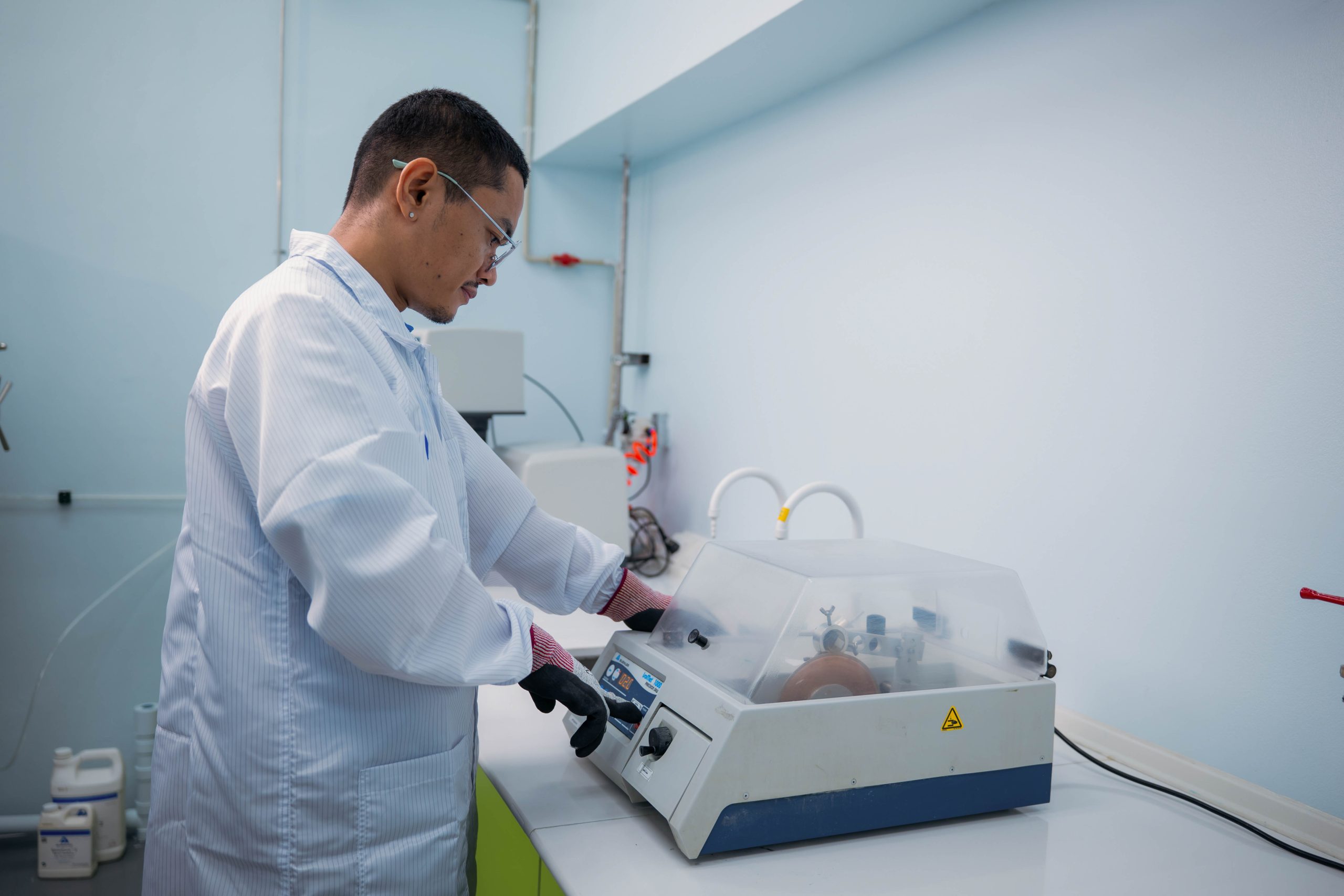
Stage 1: Sample Preparation
Document the sample Before any cutting begins, the specimen is photographed in full — capturing the overall condition and the specific area of interest. This creates a visual baseline for the entire analysis.
Precision cutting The specimen is cut using specialized equipment, maintaining a minimum distance of 1.0 cm from the region of interest to avoid cutting-induced damage. If the area is particularly sensitive, the sample is pre-mounted in epoxy resin to protect it during sectioning.
Ultrasonic cleaning The cut specimen is cleaned in an ultrasonic bath for 2–3 minutes, then thoroughly dried — removing any debris or contamination that could affect imaging quality.
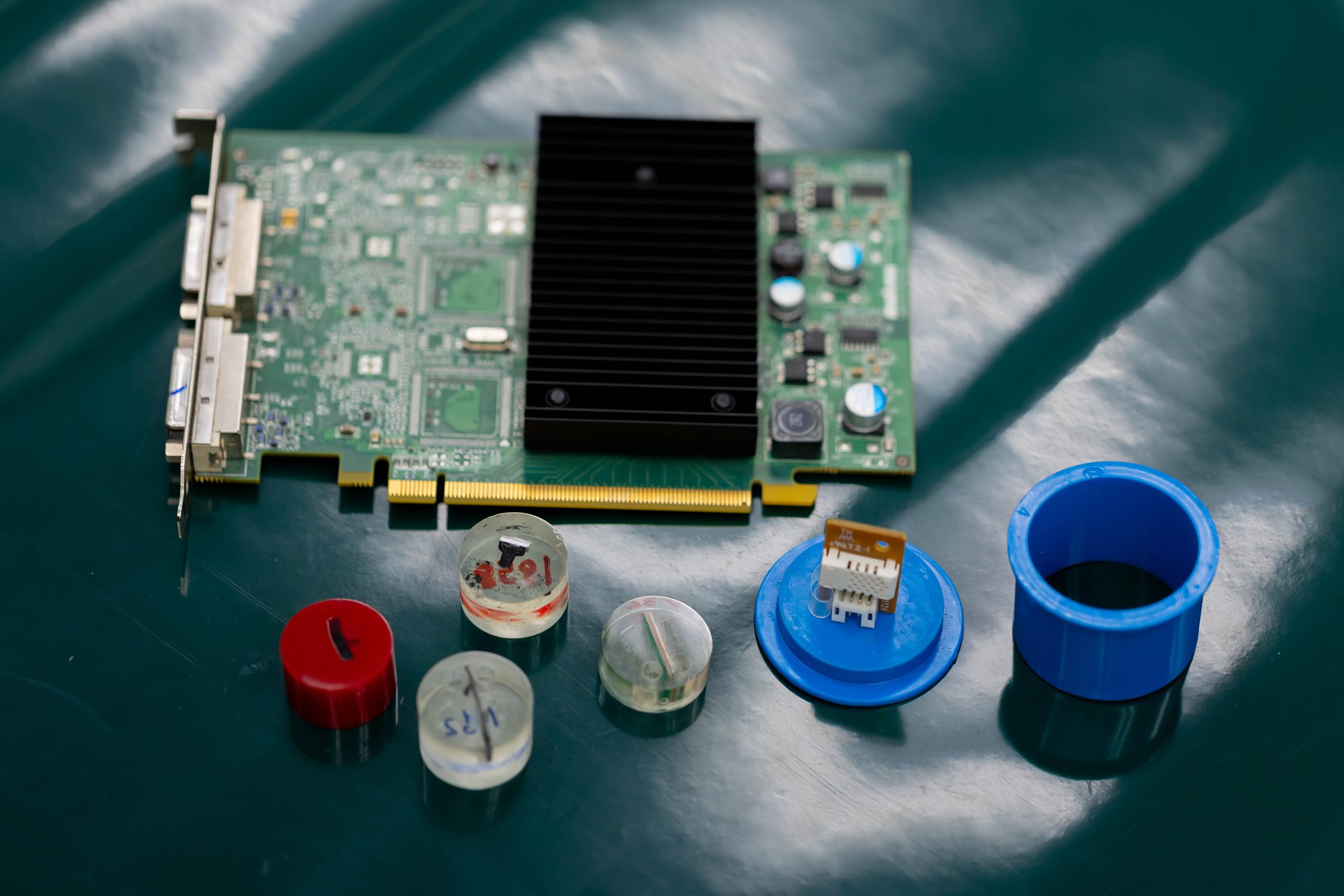
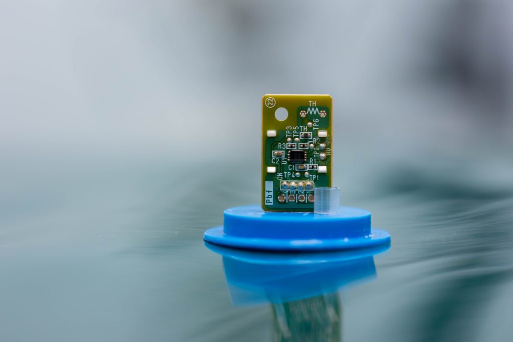
Stage 2: Mounting (Casting)
The specimen is embedded in a precisely measured mixture of epoxy resin and hardener, cast into a mold that holds it securely in the correct orientation. Once fully cured, the mounted sample is carefully removed from the casting cup.
The casting cup is cleaned with IPA-soaked cloth after each use to remove cured resin residue — maintaining consistent mounting quality across samples.
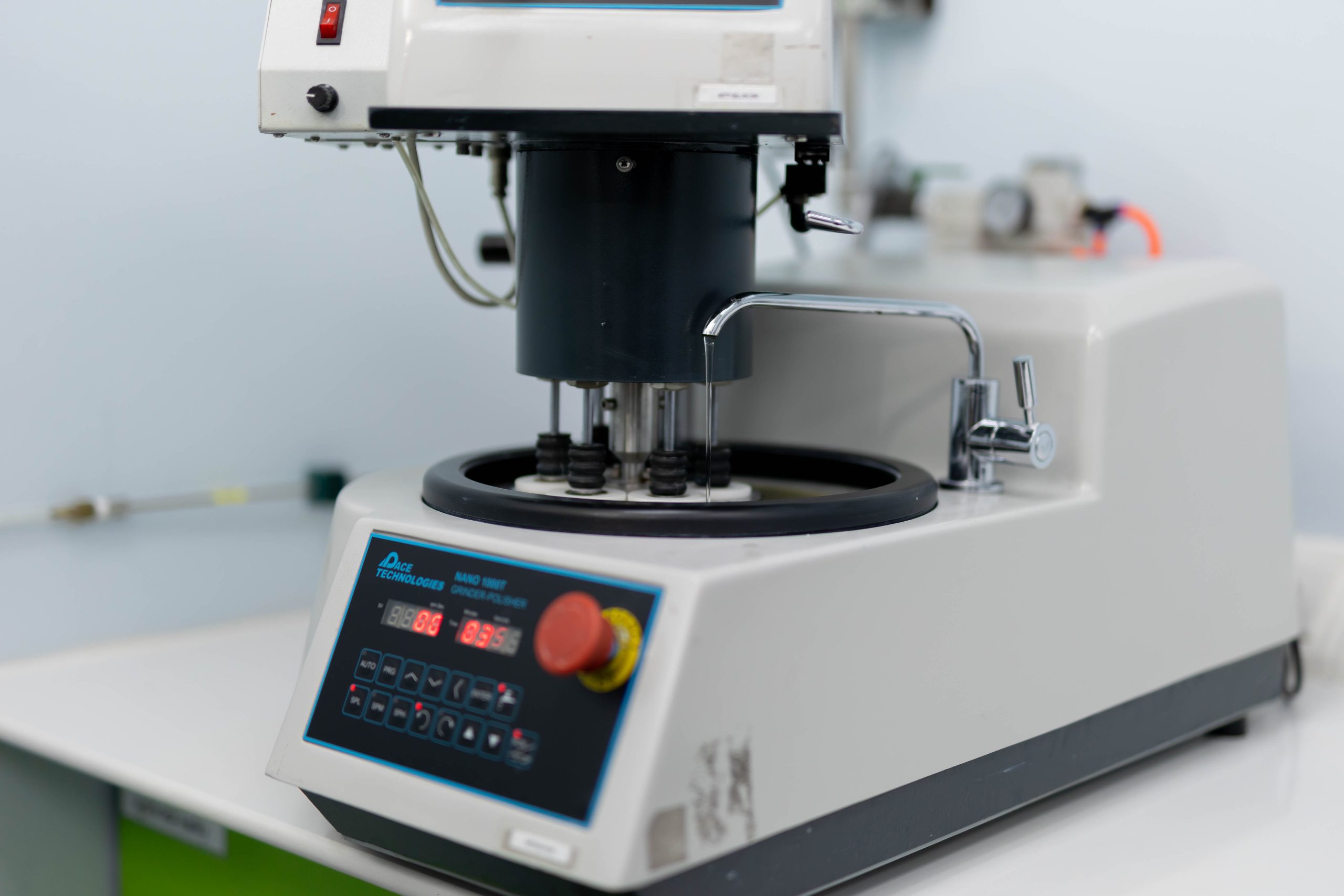
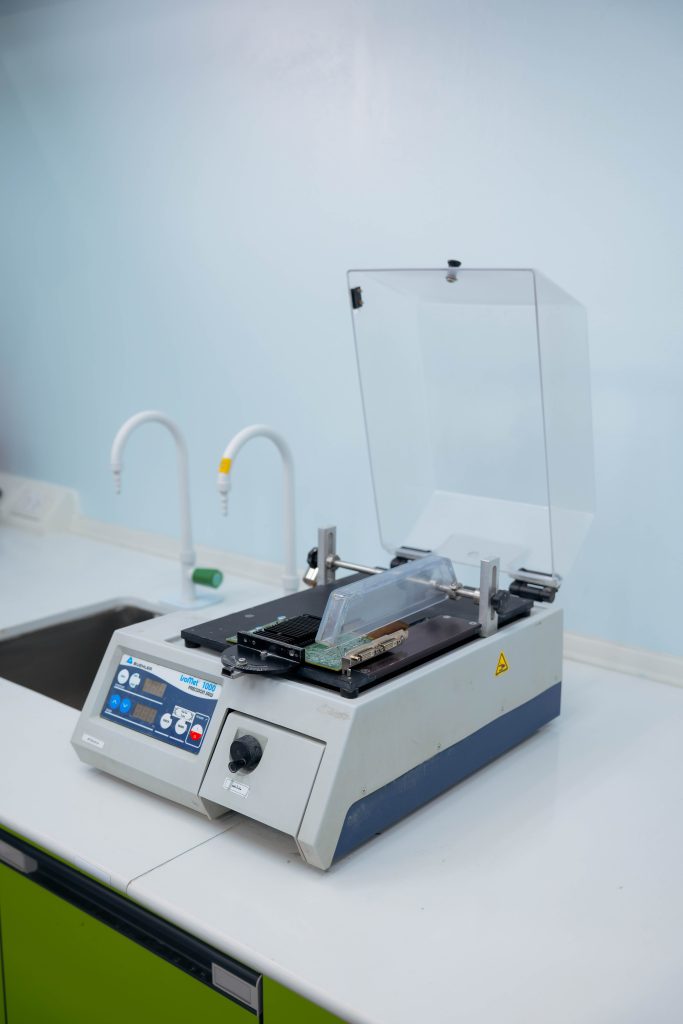
✨ Stage 3: Grinding and Polishing
The mounted specimen is processed on a NANO 1000T Grinder-Polisher, working through progressively finer abrasives at controlled speeds until the cross-section surface is perfectly flat, smooth, and ready for microscopic examination.

Stage 4: Microscopic Analysis
Optical Microscopy Using a high-performance optical microscope at magnifications ranging from 10× to 500× (selected based on sample characteristics), the cross-section is systematically imaged and examined for visible defects, layer integrity, and structural anomalies.
SEM/EDX Analysis For deeper investigation, Scanning Electron Microscopy (SEM) provides nanometer-level resolution imaging of internal structures, while Energy Dispersive X-ray Spectroscopy (EDX) identifies the elemental composition of specific areas — revealing not just where a problem exists, but what it’s made of.
Stage 5: Reporting
Analysis data — including images, measurements, and compositional findings — is compiled into a comprehensive report. Results are presented with supporting graphics, charts, and clear scientific interpretation, making findings accessible to both technical and non-technical stakeholders.
The Technical Toolkit: Key Analysis Techniques
Optical Microscopy
Uses visible light to generate high-resolution images at the micrometer scale. The standard first step for examining solder joint quality, layer continuity, and surface-level defects in PCBs and electronic assemblies.
⚡ Electron Microscopy (SEM & TEM)
Replaces light with a focused electron beam to achieve nanometer-scale resolution — far beyond what optical microscopy can deliver. Essential for studying particle morphology, interface characteristics, and fine structural details that affect electrical and mechanical performance.
️ Metallographic Analysis
Chemical etching techniques are applied to reveal grain boundaries, phase distributions, and internal microstructure in metallic materials — enabling detailed assessment of structural continuity and micro-level defects.
Hardness Testing (Vickers / Rockwell)
Quantifies the mechanical properties of materials at the cross-section — including hardness, wear resistance, and strength — providing critical data for quality certification and material performance evaluation.
X-ray Analysis (XRD & XRF)
- XRD (X-ray Diffraction) — Reveals crystal structure and phase composition of materials
- XRF (X-ray Fluorescence) — Identifies elemental composition and detects contamination or impurities
Together, these techniques provide a complete chemical and structural picture of the material under investigation.
What Materials and Applications Can Cross-Sectional Analysis Examine?


Cross-sectional analysis is far more versatile than many realize. Beyond electronics, it has applications across virtually every field of materials science and engineering:
️ Electronic Materials
- PCBs — Detecting soldering defects, delamination, via integrity issues, and layer thickness non-conformance
- Electronic components — Capacitors, resistors, and ICs: internal structural assessment and material integrity verification
Metallic Materials
- Metal alloys — Examining crystal structure, elemental distribution, and internal defects such as cracks or incomplete fusion
- Industrial materials — Evaluating mechanical properties and wear resistance of steel and aluminum for structural and machinery applications
Chemical and Polymer Materials
- Plastics and polymers — Analyzing internal structure, additive distribution, strength, and flexibility characteristics
- Ceramic materials — Assessing internal structure, fracture resistance, and impact strength for industrial ceramic applications
Medical and Biomedical Research
- Biological tissue — Studying cellular architecture, comparing cancerous and healthy cells, and evaluating tissue response to treatment
- Vaccines and pharmaceuticals — Examining structural composition to assess formulation stability and efficacy
Social Sciences
- Cross-sectional studies — Collecting population-level data at a single point in time to analyze factors influencing health outcomes, behaviors, and demographic trends — providing foundational data for longitudinal research
Why Choose ALS for Cross-Sectional Analysis?
ALS Testing combines state-of-the-art instrumentation — including high-performance optical microscopes, SEM/EDX systems, and precision grinding equipment — with years of hands-on expertise in electronics failure analysis and materials characterization.
Our ISO/IEC 17025 accredited laboratory ensures that every analysis is conducted to the highest international standards, with results that are scientifically defensible, clearly communicated, and ready to support your quality decisions.
Whether you’re investigating a field failure, validating a new manufacturing process, or developing the next generation of electronic products, cross-sectional analysis with ALS gives you the internal insight you need to get it right.
Contact ALS Testing Services (Thailand)
ALS Testing Services (Thailand) Co., Ltd. Advanced chemical analysis and materials testing — powered by modern technology and specialist expertise.
When surface inspection isn’t enough — cut deeper with ALS. Contact our team today to discuss your cross-sectional analysis requirements.