
Scanning Electron Microscopy (SEM) Analysis & How It Works and Automotive Applications

ISO 16232 vs VDA 19 & Which Automotive Cleanliness Standard Do You Need?
June 2, 2026
VOC Testing for Automotive Interiors & VDA 278, ISO 12219 and What You Need to Know
June 2, 2026Scanning Electron Microscopy (SEM) Analysis & How It Works and Automotive Applications
When an automotive component fails in the field, or returns from an OEM qualification test with an unexplained result, the investigation eventually reaches a question that cannot be answered with a magnifying glass. The fracture surface looks unusual under optical microscopy, but the relevant features are below the resolution limit. The corrosion morphology suggests a specific mechanism, but you cannot confirm it from a visual examination. A particle was found on a critical surface, but its identity and origin are unknown.
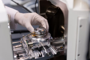
Scanning electron microscopy resolves that question. SEM is the analytical bridge between what you can observe at the macro scale and what you need to know at the micro and nano scale. It is the single most powerful imaging tool available for failure analysis work in automotive manufacturing, and it is the technique that separates a surface-level investigation from a definitive root cause conclusion.
This article explains how SEM analysis works, what makes it uniquely suited to automotive failure investigation, and the specific applications where it delivers information that no other technique can provide.
How Scanning Electron Microscopy Works
Optical microscopy uses visible light to form an image. The resolution limit of optical microscopy is set by the wavelength of light, which constrains maximum useful magnification to approximately 1,000 to 2,000 times. Beyond that limit, the image becomes blurred rather than more detailed. For many failure analysis scenarios, this is insufficient. Fatigue striations, grain boundary features, corrosion pit morphology, and the surface texture of fracture faces all occur at scales that demand higher resolution.
Scanning electron microscopy replaces the light beam with a focused beam of electrons. Electrons have a wavelength several orders of magnitude shorter than visible light, which is what allows SEM to achieve resolution several hundred times greater than optical microscopy. The practical result is that SEM can produce sharp, detailed images at magnifications from approximately 20 times up to 100,000 times or higher, with a depth of field that is far greater than optical microscopy at equivalent magnifications.
The operating principle is sequential scanning. The electron beam is rastered across the sample surface in a grid pattern. At each point, the beam interacts with the sample and generates signals that are detected and used to construct the image. The most commonly used signal in standard SEM imaging is secondary electrons, which are low-energy electrons ejected from the sample surface by the primary beam. Because secondary electron emission is highly sensitive to surface topography, secondary electron images show the three-dimensional texture of the sample surface with exceptional clarity.
A second commonly used signal is backscattered electrons, which are primary beam electrons reflected back from the sample by elastic scattering. Backscattered electron intensity is strongly dependent on the atomic number of the elements in the sample: heavier elements appear brighter and lighter elements appear darker. This makes backscattered electron imaging valuable for identifying compositional contrast across a sample surface, for example distinguishing different phases in an alloy microstructure or identifying heavy-element inclusions in a polymer matrix.
SEM gives you the surface of a component or fracture face at a scale where the failure mechanism leaves its clearest physical record. What happened to a component is written in features that are tens to hundreds of micrometres in size. SEM reads that record.
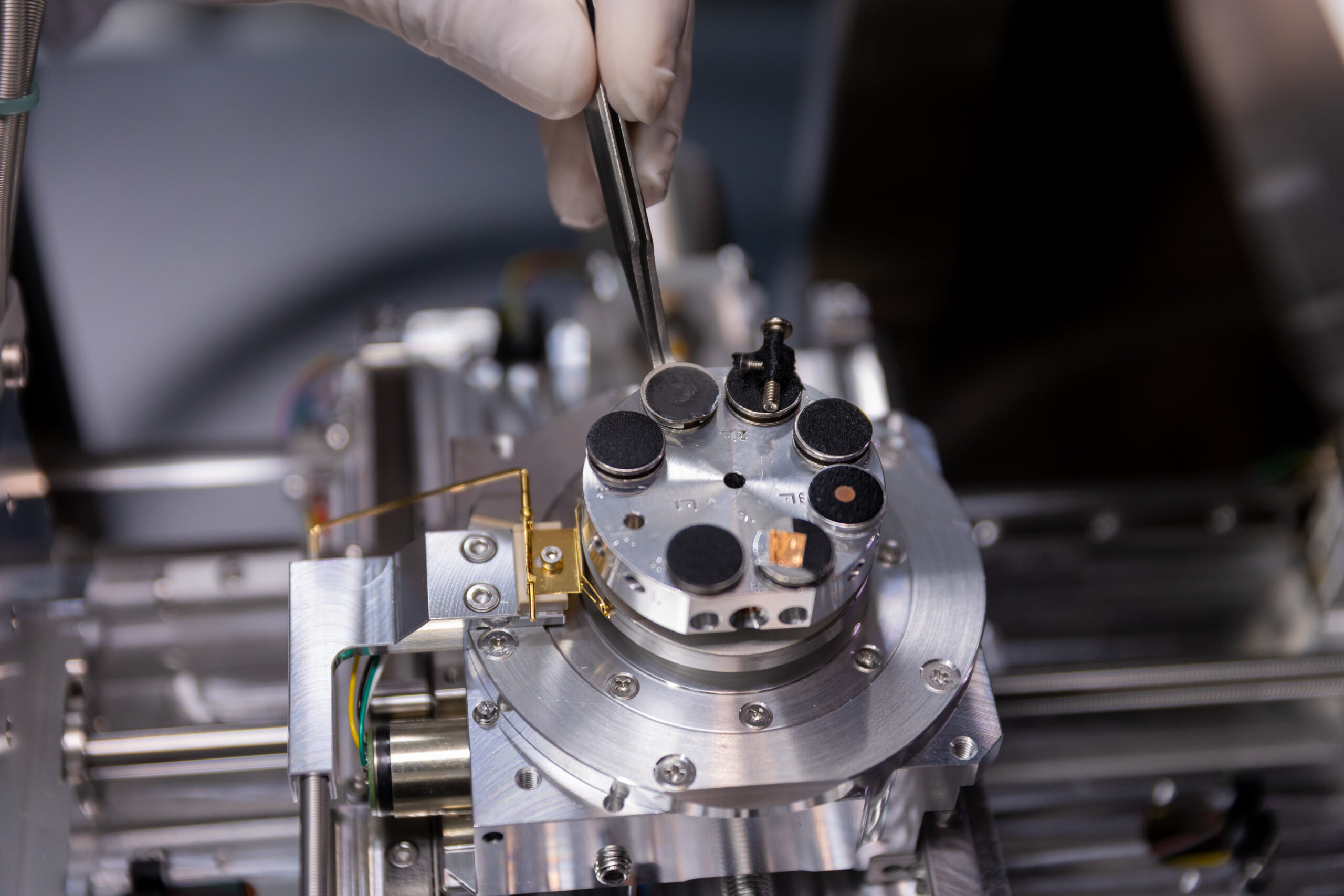
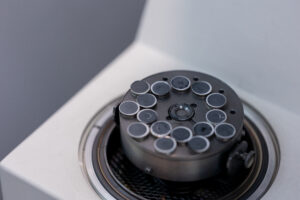
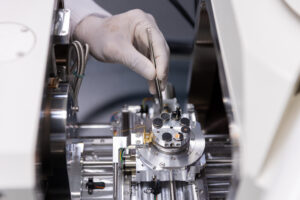
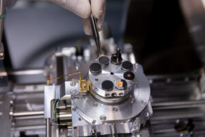
Sample Preparation for SEM
Most metallic and ceramic samples can be imaged directly in the SEM without preparation, provided they are clean and appropriately sized for the sample chamber. Non-conducting samples, including most polymers, rubber, and unfilled ceramics, require a thin conductive coating applied by sputter deposition, typically gold, platinum, or carbon, to prevent the sample surface from charging under the electron beam. Charging causes image distortion and artefacts that interfere with analysis. The coating layer is typically 5 to 20 nanometres thick and does not obscure the surface features of interest.
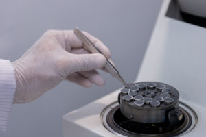
For cross-section analysis, samples are prepared by cutting through the area of interest, embedding in a low-shrinkage resin, and grinding and polishing to a metallographic finish. This reveals the internal structure of the component at the cut plane, including coating layers, grain structure, crack paths, and interface morphology, all of which can then be imaged and analysed by SEM.
Sample preparation is a critical step that directly affects the quality of SEM results. Contamination introduced during preparation, or damage to fracture surfaces from careless handling, can mask or destroy the very features the analysis is designed to reveal. Experienced analysts handle samples with this in mind from the moment of receipt.
SEM Resolution and Magnification & What the Numbers Mean in Practice
Resolution and magnification are related but distinct concepts. Magnification tells you how many times larger the image is than the object. Resolution tells you the smallest feature the instrument can distinguish as separate from its neighbour.
Modern SEM instruments achieve practical working resolution of 3 to 20 nanometres depending on the instrument type and operating conditions. For most automotive failure analysis work, working resolution of 10 to 50 nanometres is sufficient to resolve the features of interest. In practice, the resolution achieved on a real sample depends on the sample condition, the accelerating voltage used, and the detector configuration. For most failure analysis work in automotive applications, working resolution of 10 to 50 nanometres is sufficient to resolve the features of interest.
The magnification range that covers most automotive failure analysis work is from 50 times to 10,000 times. At 50 to 200 times, SEM provides overview imaging of fracture surfaces and corrosion zones that gives context before higher magnification is applied. At 500 to 2,000 times, the characteristic features of specific failure mechanisms become clearly visible: fatigue striations, cleavage facets, intergranular fracture paths, corrosion pit morphology. Above 5,000 times, fine microstructural features, nano-scale corrosion products, and the surface morphology of individual particles can be resolved.
| Magnification Range | What It Shows | Typical Application |
| 20x to 200x | Overview of fracture faces, corrosion zones, large defects | Initial characterisation, failure site mapping |
| 200x to 1,000x | Fracture morphology, crack initiation sites, gross microstructural features | Failure mechanism identification |
| 1,000x to 5,000x | Fatigue striations, cleavage facets, grain boundary details, corrosion pits | Root cause determination, mechanism confirmation |
| 5,000x to 20,000x | Fine microstructural features, corrosion product morphology, thin film details | Detailed mechanism analysis, corrosion characterisation |
| 20,000x and above | Nano-scale features, particle surface morphology, ultra-thin coating details | Advanced characterisation, research-level analysis |
SEM-EDX Combining Imaging with Elemental Analysis
SEM imaging tells you what a feature looks like. Energy-dispersive X-ray spectroscopy (EDX), also written EDS, tells you what it is made of. The two techniques are routinely operated together, using the same electron beam in the same instrument, and together they are more powerful than either technique alone.
When the primary electron beam interacts with the sample, it generates X-rays whose energies are characteristic of the elements present. Each element produces X-rays at specific, known energies: iron at 6.4 keV, aluminium at 1.49 keV, chlorine at 2.62 keV, and so on. The EDX detector measures the energy and intensity of these X-rays, producing a spectrum that identifies which elements are present and at what relative concentrations.
In automotive failure analysis, SEM-EDX is applied in three primary ways. Point analysis targets a specific feature identified in the SEM image and produces an elemental spectrum for that location. This is used to identify a corrosion product, confirm the composition of an inclusion, or characterise a contaminating particle. Area analysis averages the elemental composition across a defined region of the sample, providing a bulk compositional snapshot. Elemental mapping uses the EDX signal to construct colour-coded maps showing where specific elements are distributed across the imaged area, revealing elemental gradients, segregation, and the spatial relationship between different phases or contamination layers.
The combination of SEM morphological imaging and EDX elemental identification is the most information-dense single analytical step available in failure analysis. It simultaneously answers what happened and what it happened to.
EDX does have limitations that experienced analysts account for. It is a surface technique with a sampling depth of approximately 1 to 2 micrometres at typical operating voltages. Quantification accuracy depends on sample geometry and is less precise for light elements (below sodium in the periodic table, including carbon, nitrogen, and oxygen) than for heavier elements. For definitive quantitative analysis of light elements or trace concentrations, EDX results are confirmed by complementary techniques such as FTIR for organic identification or ICP-MS for trace elemental quantification.
For a deeper look at EDX elemental analysis and its role in failure investigation, see our dedicated EDX Analysis guide: /blog/edx-analysis/
Automotive Applications of SEM Analysis
SEM analysis is applied across a wide range of failure scenarios in automotive manufacturing and service. The following are the most significant application areas in the context of ALS’s failure analysis work.
Fracture and Fatigue Analysis
Fracture surfaces are the primary domain of SEM in automotive failure analysis. The mechanism of a fracture leaves characteristic morphological signatures on the fractured faces, and SEM imaging at appropriate magnification reveals these signatures clearly.
Fatigue fractures are identified by the presence of fatigue striations: closely spaced parallel marks that represent the crack front position at each load cycle. Striations are typically visible at magnifications of 1,000 to 5,000 times, and their spacing provides information about the crack growth rate per cycle. The initiation site of a fatigue crack is identifiable in the SEM image by the convergence of striation patterns and is typically associated with a stress concentration: a surface defect, a machining mark, a corrosion pit, or an inclusion.
Brittle fracture modes leave different signatures. Cleavage fracture in crystalline metals produces flat, faceted fracture surfaces aligned with specific crystallographic planes, visible in SEM as bright, planar areas with characteristic river line patterns. Intergranular fracture, where the crack propagates along grain boundaries rather than through grains, produces a faceted surface where individual grain surfaces are visible. This mode is associated with grain boundary embrittlement from hydrogen absorption, temper embrittlement, or grain boundary corrosion.
Ductile overload fracture produces a dimpled surface morphology at the microscale, where micro-voids nucleate at inclusions or particles and coalesce as the material deforms. The presence and size of dimples, and whether they are equiaxed or elongated, provides information about the stress state at fracture.
Corrosion Characterisation
SEM imaging characterises the morphology of corrosion damage in detail that cannot be achieved by optical microscopy. Pitting corrosion is identified by the hemispherical or crystallographic pit geometry and the presence of corrosion product deposits within and around the pits. The EDX spectrum of the corrosion products identifies the mechanism: chloride-rich corrosion products indicate chloride-induced pitting, sulfate-rich products indicate sulfuric acid attack, and the presence of zinc, chromate, or other coating elements indicates breakdown of the protective layer.
Crevice corrosion, galvanic corrosion at bimetallic interfaces, and stress corrosion cracking all have distinctive SEM signatures. Stress corrosion cracking produces branched or transgranular crack morphology that SEM distinguishes clearly from mechanical fatigue. Cross-section SEM imaging of corroded surfaces shows the depth and morphology of the corroded zone, the integrity of any remaining coating, and the relationship between the corrosion front and the underlying microstructure.
Contaminant and Particle Identification
When foreign particles are found on automotive component surfaces, in hydraulic fluids, on electrical contacts, or on PCB surfaces, SEM-EDX provides the most direct path to identification. The morphology of a particle (rounded, angular, fibrous, platelet-shaped) narrows the candidate material types. The EDX elemental composition provides positive identification: an iron-rich angular particle is consistent with machining swarf, a silicon and oxygen-rich particle suggests a silicate mineral contaminant, a carbon-rich fibrous particle indicates organic fibre contamination.
This combination of morphological and compositional information is essential for contamination source investigation. Identifying not just that contamination is present but where it likely originated from allows targeted corrective action in the manufacturing process. In cleanliness testing applications where particles are extracted from precision components and collected on filter membranes, SEM-EDX analysis of specific particles from the filter provides the particle identification data required by some OEM cleanliness specifications and by failure investigations where particle composition is central to the root cause.
Coating and Surface Treatment Analysis
SEM cross-section analysis is the primary tool for characterising the thickness, morphology, and integrity of coatings, platings, and surface treatments on automotive components. A properly prepared cross-section through a coated surface reveals each layer in the coating stack with nanometre-scale detail: the base material microstructure, the interface between base material and coating, each individual coating layer and its thickness uniformity, and any defects such as porosity, cracking, or delamination planes within the coating.
EDX line scan analysis across the cross-section shows how the elemental composition transitions from one layer to the next, identifying the composition of each layer and detecting diffusion zones, interdiffusion effects, or contaminating species at layer interfaces. This is particularly relevant for investigation of adhesion failures, where the locus of failure (whether it occurred within a layer or at an interface) determines whether the failure is a coating process problem, a surface preparation problem, or a design problem.
PCB and Automotive Electronics Failure Analysis
Electronic components and PCB assemblies in automotive applications are subject to increasingly stringent reliability requirements, driven by the safety-critical nature of automotive control systems. SEM analysis is central to failure investigation in this domain.
Solder joint failures are characterised by SEM to distinguish fatigue-driven cracking from brittle intermetallic fracture, from dewetting and non-wet opens caused by poor solderability. The fracture morphology and the composition of the solder and intermetallic layers identified by EDX provide the evidence to determine root cause. Corrosion and dendritic growth failures on PCB surfaces are investigated by SEM to characterise the morphology of the corrosion product and identify the ionic species responsible through EDX analysis. The distribution and density of corrosion sites across the board provides information about whether contamination was local or global, which guides the corrective action.
For PCB ionic contamination analysis and chemical cleanliness investigation, see our Chemical and Electronics Testing services: https://www.alstesting.co.th/anion-test-specialist-malaysia/
SEM vs Optical Microscopy & When to Use Each
SEM and optical microscopy are complementary techniques. In a structured failure analysis investigation, both are used, with optical microscopy providing the initial characterisation and SEM providing the higher-resolution detail needed to reach a definitive conclusion.
| Dimension | Optical Microscopy | SEM Analysis |
| Maximum useful magnification | 1,000x to 2,000x | Up to 100,000x or higher |
| Resolution | 0.2 micrometres (diffraction limited) | Typically 3 to 20 nm (varies by instrument/settings) |
| Depth of field | Low – challenging for rough fracture surfaces | High – excellent for three-dimensional surfaces |
| Colour imaging | Yes – colour information from reflected light | No – greyscale images only (BSE gives compositional contrast) |
| Elemental analysis | Not available | Available via EDX – point, area, and map |
| Sample preparation | Minimal for most samples | Coating required for non-conducting samples |
| Throughput | Fast – rapid overview imaging | Slower – higher setup time per sample |
| Best application | Initial survey, large-area overview, surface colour assessment | High-resolution characterisation, elemental identification, fine feature analysis |
| Cost | Lower per hour | Higher per hour – more information per analysis |
The practical workflow in failure analysis begins with stereo microscopy for large-area overview and failure site identification, moves to optical microscopy for initial characterisation at intermediate magnifications, and then applies SEM for the high-resolution imaging and EDX elemental analysis that establishes root cause. This sequence preserves the most informative analytical steps and ensures that SEM time is focused on the features that matter most.
What SEM Analysis Cannot Do
Understanding the limitations of SEM is as important as understanding its capabilities. SEM is an imaging and elemental analysis technique. It is not a molecular identification technique: it can tell you that a particle contains carbon, oxygen, and iron, but it cannot tell you whether the organic phase is a polyamide, a polyester, or an epoxy. For molecular identification of organic materials, FTIR spectroscopy is the appropriate complementary technique.
SEM is also a surface technique. Without cross-section preparation, it analyses only the surface of the sample. Subsurface features, internal cracks, and through-thickness compositional gradients are not visible in surface SEM imaging without sectioning. For volumetric characterisation, techniques such as serial cross-section analysis or X-ray computed tomography (available at specialist facilities) are required.
EDX quantification is more accurate for heavier elements than for light elements. Carbon, nitrogen, and oxygen are detectable but quantified with lower accuracy than elements from sodium and above in the periodic table. When precise quantification of light elements is required, complementary techniques including combustion analysis or carrier gas hot extraction are used.
These limitations are not reasons to avoid SEM. They are reasons to use it as part of a structured, multi-technique failure analysis programme where each technique’s output builds on and is corroborated by the others.
SEM Analysis at ALS Testing
ALS Testing provides SEM and SEM-EDX analysis as part of our automotive failure analysis services. Our SEM capability covers the full range of applications described in this article: fracture and fatigue analysis, corrosion characterisation, contaminant and particle identification, coating cross-section analysis, and PCB and electronics failure investigation.
All SEM analysis at ALS is conducted within our ISO/IEC 17025:2017 accredited quality management system, with documented equipment calibration, analyst qualification records, and sample traceability throughout. Our reports include representative SEM images with scale bars, magnification data, and operating conditions, supported by EDX spectra and maps where elemental characterisation is part of the investigation scope. Reports are formatted to support OEM submission, warranty dispute documentation, and technical engineering review.
Our failure analysis team has experience across the full range of automotive materials and component types: metals, polymers, composites, coatings, adhesives, and electronics assemblies. When a failure reaches the SEM stage, we have the context and the technical depth to connect what we see in the image to what was happening in the manufacturing process or service environment.
Summary
Scanning electron microscopy is the central imaging tool of automotive failure analysis. It achieves magnifications and resolutions that optical microscopy cannot reach, with a depth of field that makes it uniquely suited to imaging the rough, three-dimensional surfaces of fractures and corrosion zones. When combined with EDX elemental analysis, it identifies not just the morphology of a failure feature but the material it involves.
In automotive applications, SEM analysis is applied to fracture and fatigue investigation, corrosion characterisation, contaminant and particle identification, coating and surface treatment analysis, and PCB and electronics failure investigation. It is the technique that converts a visible failure into a defensible root cause conclusion, supported by documented images and data that hold up in OEM review, warranty proceedings, and regulatory submissions.
Next Steps
See our Failure Analysis services and full SEM capability overview: https://www.alstesting.co.th/failure-analysis-services-sem-ftir-edx-als-testing/
Read our guide to EDX elemental analysis in failure investigation: /blog/edx-analysis/
For PCB and electronics failure analysis including ionic contamination: https://www.alstesting.co.th/anion-test-specialist-malaysia/
Contact our team to discuss a failure investigation: https://www.alstesting.co.th/contact-us/